
Larger photomasks could increase production capacity for high-end chips and RAM.
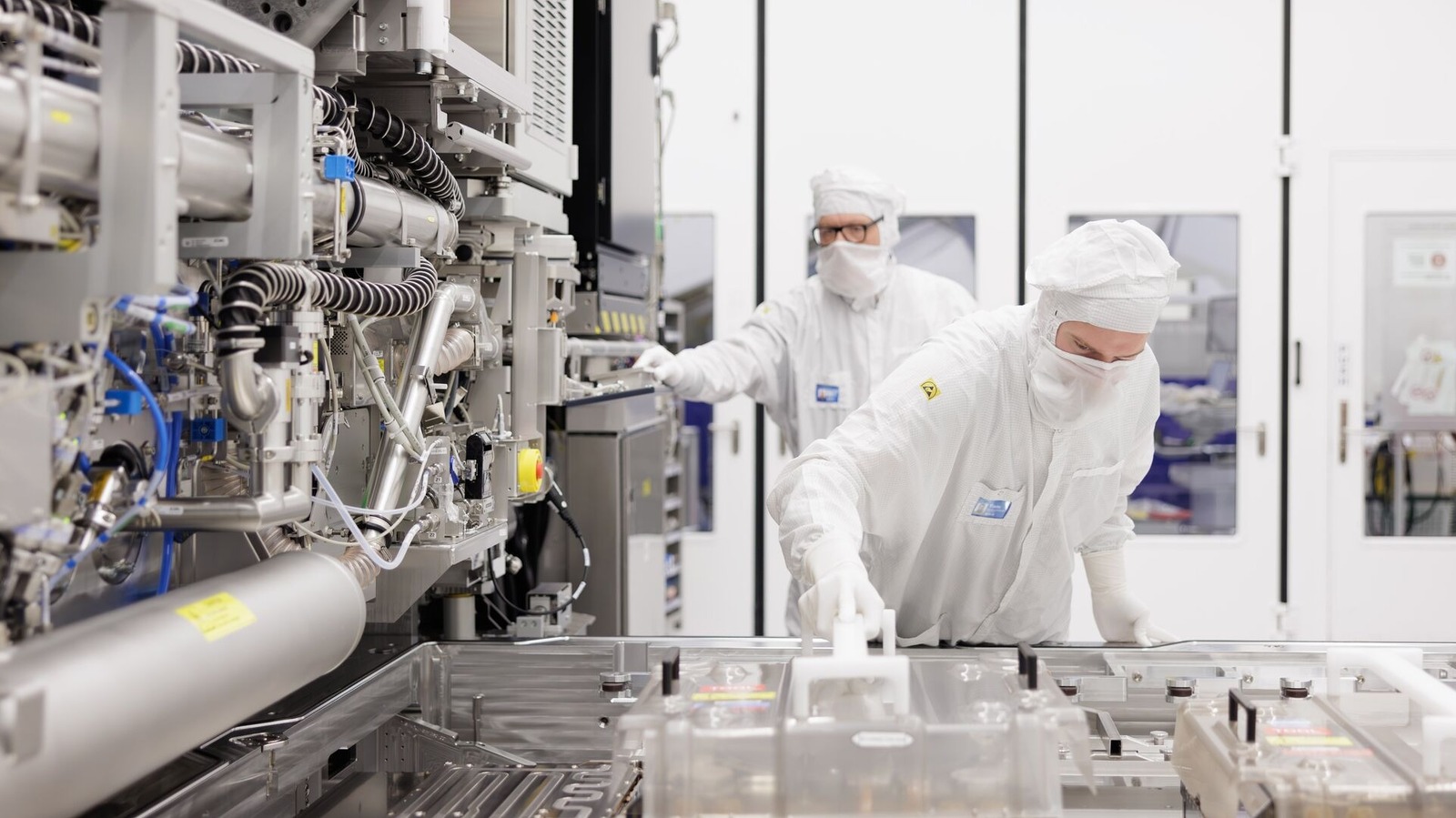
Samsung and TSMC will join Intel in adopting ASML's latest High NA extreme ultraviolet (EUV) lithography chip fab machines, ASML announced. The three companies also unveiled a new initiative to adopt larger 12-inch photomasks that will hopefully boost manufacturing yields and lower chipmaking costs. Samsung and TSMC will deploy ASML's NA EUV tech by 2028 and 2030 respectively, while 12-inch photomasks are expected to arrive in advanced node production by 2033.
Currently, ASML's High NA EUV technology has only been deployed by Intel on its 18A process for select Core Ultra Series 3 (Panther Lake) processors. The company is also working on an advanced version called 18A-P, under consideration by Apple for its next-gen A-series iPhone processors. Today, ASML boasted that Intel has built more than a million wafers using the new process.
Now, both TSMC and Samsung, the world's number one and two chip manufacturers, have committed to the High NA EUV tech as well. Samsung plans to build DRAM memory products using NA EUV by 2028, while TSMC said it will deploy the tech in advanced nodes starting in 2030. As Intel showed, though, ramping up to the tech is not that easy and both companies may run into bottlenecks that thwart their planned production dates.
ASML also announced that it has created an initiative with TSMC and Samsung to transition to large-format 12-inch photomasks — used to "stencil" chip patterns onto wafers — from the current standard of six inches. Another large chipmaker, SK Hynix, is evaluating its own participation in the consortium. The larger masks will "increase fab productivity, lower chipmaking costs and remove stitching constraints," TSMC noted.
The new masks will allow companies to print the finer features of the NA EUV process onto larger chips. Currently, processors made with this process must have features "stitched" together, something that adds complexity and cost to the manufacturing process. The 12-inch photomasks will allow fabs to make those chips without stitching, reducing cost and complexity.
ASML will start testing 12-inch photomask fabs in 2031, with production expected to start in 2033. "If we're going to pull it off as an industry, then you'll actually see that the productivity of those systems will go up by 40 percent," ASML's chief technology officer Marco Pieters told Reuters.